|
|
|
||||||||||||||||||||


|
|||||||||||||||||||


 물품구매안내")


 톡톡
톡톡- 모터, 서보모터, 스텝모터 드라이버 및 컨트롤러
-
[로봇사이언스몰][Pololu][폴로루] DRV8874 Single Brushed DC Motor Driver Carrier #4035
상품번호 : 19417 아이콘 설명보기
![[로봇사이언스몰][로봇사이언스몰][Pololu][폴로루] DRV8874 Single Brushed DC Motor Driver Carrier #4035>>모터, 서보모터, 스텝모터 드라이버 및 컨트롤러](/data/goods/1/2022/05/19417_temp_16537105715187view.jpg)
![[로봇사이언스몰][로봇사이언스몰][Pololu][폴로루] DRV8874 Single Brushed DC Motor Driver Carrier #4035>>모터, 서보모터, 스텝모터 드라이버 및 컨트롤러](/data/goods/1/2022/05/19417_temp_16537105714820view.jpg)


This compact breakout board for TI’s DRV8874 motor driver offers a wide operating voltage range of 4.5 V to 37 and can deliver a continuous 2.1 A (6 A peak) to a single bidirectional brushed DC motor. The DRV8874 also features integrated current sensing and regulation as well as built-in protection against under-voltage, over-current, and over-temperature. The carrier board adds protection against reverse voltage.
 Compare all products in Brushed DC Motor Drivers.
Description
Overview
This product is a carrier board for Texas Instruments’ DRV887x family of motor drivers; we therefore recommend careful reading of the corresponding driver’s datasheet before using this product. Three pin-compatible versions are available that differ in the amount of current they can deliver while supporting the same 4.5 V to 37 V operating voltage ranges and control interfaces.
Details for item #4035
This carrier for TI’s DRV8874PWP motor driver can supply continuous currents up to approximately 2.1 A and can tolerate peak currents up to 6 A. Since this board is a carrier for the DRV8874, we recommend careful reading of the DRV8874 datasheet. The board ships populated with all of its SMD components, including the DRV8874.

Features

Using the motor driver

Motor and motor power connections are made on one side of the board and logic power and control connections are made on the other. The driver requires a motor voltage between 4.5 V and 37 V to be supplied to the VIN or VM pin. The driver is in sleep mode by default, and a logic voltage between 1.8 V and 5.5 V must be supplied to the SLEEP pin; to take it out of sleep mode. This logic voltage can typically shared with the controlling device, or it can be supplied by an output from the controlling device, which allows for dynamic control of the sleep mode. The VIN pin is the reverse-protected motor supply input and is the recommended point for connecting motor power. VM is an access point for motor supply power after the reverse voltage protection circuit.
The DRV8874/DRV8876 features three possible control modes: phase/enable (PH/EN), PWM (IN/IN), and independent half-bridge. The PMODE pin determines the control interface, and the state is latched when the driver is enabled through the SLEEP pin.
Phase/enable (PH/EN) mode
Setting the PMODE pin low prior to enabling the driver, as shown in the diagram above, sets the driver to phase/enable control mode, where the PH pin determines the motor direction and the EN pin can be supplied with a PWM signal to control the motor speed (this is typically referred to as sign-magnitude operation). This mode is generally easier to use as it only requires one PWM signal, but it only allows for drive/brake operation. (Drive/brake operation usually provides a more linear relationship between PWM duty cycle and motor speed than drive/coast operation, and we generally recommend using drive/brake operation when possible.)
| Simplified drive/brake operation with PMODE=0 (PHASE/ENABLE) | ||||
|---|---|---|---|---|
| EN | PH | OUT1 | OUT2 | operating mode |
| 0 | X | L | L | brake low (outputs shorted to ground) |
| PWM | 1 | PWM (H/L) | L | forward/brake at speed PWM % |
| PWM | 0 | L | PWM (H/L) | reverse/brake at speed PWM % |
This mode can also be used for locked-antiphase operation, where a sufficiently high-frequency (up to 100 kHz) PWM is applied to the phase (PH) pin and the enable (EN) pin is tied high. In locked-antiphase operation, the PWM duty cycle controls speed and direction, going from full-speed in one direction at 0% duty cycle to full speed in the other direction at 100% duty cycle. A duty cycle of 50% will stop the motor. The appropriate PWM frequency will generally depend on the inductance of the motor.
Advanced usage with PWM (IN/IN) mode

When the PMODE pin is set high prior to enabling the driver, the driver is set to PWM (IN/IN) control mode, which allows for more advanced control options, including allowing the H-bridge to enter a high-impedance (coast) state without having to put it to driver sleep. The following truth table show how to achieve drive/coast (slow decay) and drive/brake (fast decay) operation using the IN/IN control interface:
| PWM control mode with PMODE=1 (IN/IN) | ||||
|---|---|---|---|---|
| IN1 | IN2 | OUT1 | OUT2 | operating mode |
| 0 | 0 | Z | Z | coast (outputs off) |
| PWM | 0 | PWM (H/Z) | PWM (L/Z) | forward/coast at speed PWM % |
| 0 | PWM | PWM (L/Z) | PWM (H/Z) | reverse/coast at speed PWM % |
| PWM | 1 | L | PWM (L/H) | reverse/brake at speed 100% − PWM % |
| 1 | PWM | PWM (L/H) | L | forward/brake at speed 100% − PWM % |
| 1 | 1 | L | L | brake low (outputs shorted to ground) |
Advanced usage with independent half-bridge mode
When the PMODE pin is left high-impedance (i.e. floating or disconnected) when the driver is enabled, the driver is set to independent half-bridge control mode. See the DRV8874/DRV8876 datasheet for more information about this control mode.
Pinout


| PIN | Default State | Description |
|---|---|---|
| VIN | 4.5 V to 37 V board power supply input. | |
| GND | Ground connection points for the motor and logic supplies. The control source and the motor driver must share a common ground. | |
| VM | This pin gives access to the motor power supply after the reverse-voltage protection MOSFET (see the board schematic below). It can be used to supply reverse-protected power to other components in the system. | |
| OUT1 | Motor output 1. | |
| OUT2 | Motor output 2. | |
| EN/IN1 | LOW | Motor control input 1 (functions as an enable pin in PHASE/ENABLE mode). |
| PH/IN2 | LOW | Motor control input 2 (functions as a direction pin in PHASE/ENABLE mode). |
| PMODE | FLOATING | Control interface select pin. The state of this pin is latched when the driver is enabled through the SLEEP pin. Setting this pin low prior to enabling sets the driver to phase/enable (PH/EN) control mode. Setting this pin high prior to enabling sets the driver to PWM (IN/IN) control mode. Leaving this pin floating or disconnected on enable sets the driver to independent half-bridge control mode. |
| SLEEP | LOW | Sleep input that puts the driver into a low-power sleep mode when low. The driver outputs are high-impedance (coast) in sleep mode. |
| VREF | Current limiting threshold reference voltage (see below). | |
| IMODE | PULLED LOW | Four-state input for current regulation and overcurrent protection mode (see below). This carrier pulls down IMODE to GND through a 20 kΩ resistor setting the current chopping mode to cycle-by-cycle, the over-current response to automatic retry, and FAULT response to current chopping and over-current. |
| FAULT | FLOATING | Open-drain, active-low fault output. This pin goes low during an over-current, over-temperature, or under-voltage condition. An external pull-up resistor is required to use this pin. |
| CS | Current sense output. This pin provides an analog current-sense feedback voltage of approximately 1.1 V/A (DRV8874) or 2.5 V/A (DRV8876). |
Current limiting
The DRV8874/DRV8876 can be configured to actively limit the current through the motors by using a fixed off-time PWM current regulation (current chopping) or a cycle-by-cycle PWM current chopping scheme. The current chopping scheme and over-current response is selectable through the IMODE quad-level input. This carrier pulls down IMODE to GND through a 20 kΩ resistor, setting the current chopping mode to cycle-by-cycle. The current limit is determined by the voltage on the VREF pin, which this carrier board pulls up to SLEEP through a 10 kΩ resistor, and the resistor on the CS pin, which this carrier board pulls down to GND through a 2.49 kΩ resistor. When SLEEP is connected to 5 V, the current limit is set to approximately 4.4 A on the DRV8874 carrier or 2 A on the DRV8876 carriers. The current limit can be lowered by connecting an additional resistor between VREF and GND or by connecting an external reference voltage directly to VREF; the current limit can be increased by connecting an additional resistor between CS and GND. Current limiting can be disabled by connecting CS directly to GND. Refer to the DRV8874/DRV8876 datasheet for more information about the driver’s current regulation.
Real-world power dissipation considerations
The DRV8874 is rated for a peak current of 6 A and the DRV8876 is rated for a peak current of 3.5 A by their respective datasheets. However, the chips by themselves will overheat at lower currents. In our tests, we found that the chips on our carrier boards were able to deliver their rated peak currents for less than a second before their thermal protections kicked in and disabled the motor outputs. They were able to operate at their default current limits of 4.4 A (DRV8874) and 2 A (DRV8876) for a few seconds before thermal shutdown. The continuous current specifications we provide for these products of 2.1 A (DRV8874 carrier), 1.3 A (DRV8876 carrier), and 1.1 A (DRV8876 (QFN) carrier) are currents we found to be sustainable for many minutes without triggering thermal shutdown. These tests were conducted at room temperature in open space with no additional cooling (e.g. no forced airflow or heat sinks).
The actual current you can deliver will depend on how well you can keep the motor driver cool. The carrier’s printed circuit board is designed to help with this by drawing heat out of the motor driver chip. PWMing the motor will introduce additional heating proportional to the frequency.
This product can get hot enough to burn you long before the chip overheats. Take care when handling this product and other components connected to it.
Included hardware


Breakaway 0.1″ male headers are included with the DRV8874/DRV8876 motor driver carriers, which can be soldered in to use the driver with perfboards, breadboards, or 0.1″ female connectors. (The headers might ship as a single larger strip that can be broken into smaller pieces.) When used with these header pins, the board can be oriented with the parts visible, as shown in the right picture above, or with the silkscreen visible, by soldering the headers in from the opposite side. You can also solder your motor leads and other connections directly to the board.
Schematic

Dimensions
| Size: | 0.6″ × 0.7″ |
|---|---|
| Weight: | 0.9 g1 |
General specifications
| Motor driver: | DRV8874 |
|---|---|
| Motor channels: | 1 |
| Minimum operating voltage: | 4.5 V |
| Maximum operating voltage: | 37 V |
| Continuous output current per channel: | 2.1 A |
| Peak output current per channel: | 6 A |
| Current sense: | 1.13 V/A |
| Maximum PWM frequency: | 100 kHz |
| Minimum logic voltage: | 1.8 V |
| Maximum logic voltage: | 5.5 V |
| Reverse voltage protection?: | Y |
| Header pins soldered?: | N |
Identifying markings
| PCB dev codes: | md41a |
|---|---|
| Other PCB markings: | 0J13404 |
Notes:
File downloads
Recommended links
 아이콘이 부착된 상품
 b. 해외상품 :
1) 해당상품:  아이콘이 부착된 상품
2) 구매금액 700,000원 이상 : 입금확인 후 최소 5일 ~ 최대 2주
3) 구매금액 700,000원 이하 : 입금확인 후 최소 1주 ~ 최대 8주
4) 단, 해외계약업체에 품절되지 않은 상품에 한함
② 구매상품 종류가 많을 경우 예상 준비기간 보다 더 소요 될 수 있습니다.
③ 주문하신 상품은 출고완료 메일 또는 문자 수신 후 익일~최대7일(도서,산간지역)
이내에 수령하실 수 있습니다.
④ 제주(\3,500원)/도서지역(\5,000원)은 배송비가 추가됩니다.
제주,도서, 산간지역은 타 지역보다 배송기간이 길어질 수 있습니다.
⑤  아이콘이 부착된 상품이라도 국내재고가 있을 수 있습니다.
⑥ 해외 현지 사정으로 인해 공지한 배송기간보다 더 길어 질 수 있습니다.
⑦ 해외상품은 반품/교환/취소가 어려울 수 있으니 신중히 주문하시기 바랍니다.
3. 소비자의 단순변심/착오구매에 의한 청약철회제한안내
① 전자상거래 등에서의 소비자보호에 관한 법률 제17조 제2항 및 동 시행령
제21조에 의한 청약철회 제한 사유에 해당하는 경우 및 기타 객관적으로
이에 준하는 것으로 인정되는 경우에 한합니다.
② 소비자의 단순변심, 착오구매에 의한 교환/반품 시에 발생하는 배송비는
소비자가 부담합니다.
③ 판매자의 실수,제품하자 등의 사유로 인한 배송비는 판매자가 부담합니다.
4. 상품의 교환/반품/보증조건 및 품질보증기준안내
① 상품이 공급된 날(배송완료일)로부터 7일 이내에 교환/반품을 신청 할 수 있습니다.
그러나 아래의 사유에 해당 하는 경우에는 교환/반품 신청이 받아들여지지 않을 수도 있습니다.
a. 소비자의 책임으로 인해 상품이 훼손/멸실 된 경우(확인을 위한 포장훼손제외)
b. 소비자의 사용에 의해 상품의 가치가 현저하게 감소한 경우
c. 시간의 경과로 인해 상품의 재판매가 불가하게 된 경우
d. 판매방식의 특성으로 판매자에게 회복할 수 없는 피해가 발생한 경우 (주문제작 상품, 청약철회상품 등)
② 교환/반품/보증조건 및 품질보증기준은 『소비자기본법』에 따른 소비자분쟁해결기준에 따라 피해를 보상합니다.
5. 소비자피해보상 처리, 재화 등에 대한 불만 및 분쟁처리 안내
관련상품
-
![[로봇사이언스몰] 메이커스: 어른의 과학 Vol.06 이공계 연구소 보드게임](/data/goods/1/2022/10/20106_temp_16655616023677view.png)


- [로봇사이언스몰] 메이커스: 어른의 과학 Vol.06 이공계 연구소 보드게임
- 이과생 마음 두근거리게 하는, 과학자가 만든 과학자 되어보기 보드게임
- 판매가 ₩ 78,000
-
 1,432
1,432
-
- 조건부 무료배송
-
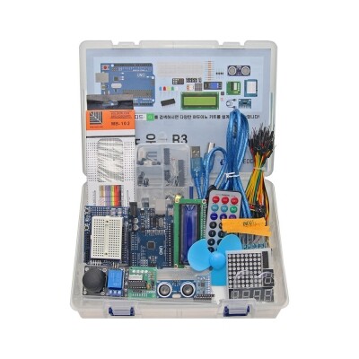
- 아두이노 우노 R3 고급 키트
- 아두이노 실습을 위한 필수 부품이 포함된 키트, 아두이노 코딩 배우기 교재가 제외된 상품입니다.
- 판매가 ₩ 65,340
-
6,662
-
- 조건부 무료배송
-
![[로봇사이언스몰][코딩로봇] 알파 미니 (ALPHA MINI)](/data/goods/1/2020/06/15334_tmp_32a415fdf174c952317188293d01b0684901view.jpg)
- [로봇사이언스몰][코딩로봇] 알파 미니 (ALPHA MINI)
- 로봇을 활용한 재미있는 코딩학습
- 판매가 ₩ 1,250,000
-
9,999+
-
- 조건부 무료배송
-
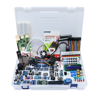
- 라즈베리파이 고급 키트
- 다양한 입출력-센서-디스플레이-통신-인터페이스 모듈 및 기타 액세서리로 구성된 울티메이트 라즈베리파이 키트
- 판매가 ₩ 99,000
-
1,870
-
- 조건부 무료배송
판매자 관련상품
-
- [로봇사이언스몰][코딩로봇] 알파 미니 (ALPHA MINI)
- 로봇을 활용한 재미있는 코딩학습
- 판매가 ₩ 1,250,000
-
9,999+
-
- 조건부 무료배송
-
- [로봇사이언스몰] 메이커스: 어른의 과학 Vol.06 이공계 연구소 보드게임
- 이과생 마음 두근거리게 하는, 과학자가 만든 과학자 되어보기 보드게임
- 판매가 ₩ 78,000
-
1,432
-
- 조건부 무료배송
-
![[로봇사이언스몰][블루이노] 스마트팜 인공지능 키트](/data/goods/1/2021/05/17457_temp_16218314494856view.png)
- [로봇사이언스몰][블루이노] 스마트팜 인공지능 키트
- 인공지능이 가미 된 내가 직접 스마트팜을 구축하고 식물을 키워볼 수 있는 키트입니다.
- 판매가 ₩ 638,000
-
9,999+
-
- 조건부 무료배송
-
![[로봇사이언스몰][교육용드론][CoDrone] 코드론 미니](/data/goods/1/2020/01/14879_tmp_f6cf2ca48125c96d1f029e73a51f1bd87855view.png)
- [로봇사이언스몰][교육용드론][CoDrone] 코드론 미니
- 코딩이 가능한 미니드론/안정적 군집 비행 3대
- 판매가 ₩ 99,000
-
9,999+
-
- 조건부 무료배송
판매자 정보
| 판매자 | 본사 | 셀러등급 | |
|---|---|---|---|
| 상호명 | (주)위키모바일(로봇사이언스몰) | 대표자 | 김경식 |
| 사업자등록번호 | 215-87-14086 | 통신판매신고번호 | 제2008-서울송파-0867호 |
| 연락처 | 02-2283-1300 | 사업장 소재지 | 서울특별시 송파구 문정동 643-1 엠스테이트 B동704호 |
2. 해외구매 특성상 주문에서 배송까지는 평균 10~15일이 소요됩니다. 간혹 현지 제품 수급에 따라 부득이하게 시일이 더 소요 될 수 있으니 구매시 좀 더 여유있게 주문하시길 권합니다.
3. 해외 내수품인 관계로 A/S에 대해서는 별도의 책임을 지지 않습니다.
4. 해외배송 특성상 주문접수후 배송상태가 배송준비중으로 넘어간 경우 해외에서 국내로의 배송이 이루어지고 있다는 뜻입니다. 따라서 배송준비중으로 배송상태가 넘어간 경우 취소및 반품이 불가하므로 이점 양해 부탁드립니다.
5. 타 해외구매대행 사이트에서 주문하신 물건과 주문날짜가 겹치지않도록 주의해 주십시오. 통관날짜가 같을 경우 합산관세가 부가되게 됩니다.